

What's so special about "integration" anyways?
There’s an unsung hero that drove most of the rapid technological growth over the last 50 years: Integration. It’s a term that on the surface can feel unimportant. So, what if circuits are integrated? How does integrating different devices together drive electronic complexity and, as a result, innovation? To answer these questions, and to understand why integration has been and will continue to be a driving force in semiconductors and therefore further technology growth advances, we have to go back in time to the beginnings of the electronics revolution and examine the recurring theme: “Integration enables new levels of complexity and performance”.
Far back in time: the Vacuum Tube
The vacuum tube was invented in 1904 and enabled the first commercial electronic systems. A vacuum tube is similar to a transistor in that you could control one or more electrical signals using a 2nd set of electrical signals. They were relatively cheap, easily replaceable, and incredibly advanced for their time with one glaring downside: they burnt out quickly like incandescent lightbulbs do. This meant that they had a fixed lifetime before the user had to replace them. Nonetheless, vacuum tubes were widely adopted. The first vacuum tubes were quite simple: they contained only 2 or 3 pins (diode or triode) and performed simple rectification/amplification tasks. When circuit designers got their hands on these new vacuum tubes, they started to conceive different ways of connecting them together to perform more complex tasks. However, combining a bunch of vacuum tubes and assembling them on a board was not a viable solution, as the tubes would randomly burn out at different times. Adding more and more tubes would mean end users were constantly replacing burnt out tubes in their electronics. So instead, the vacuum tube manufacturers started to make single vacuum tubes that performed the same functions as multiple vacuum tubes wired together. These new complex tubes, like dual pentode and triple triode tubes, enabled new functionality in a single package. Some may consider this the birthplace of integration in electronics. Now, system designers could select from a wide array of highly complex tubes that performed various functions leading to greater circuit complexity and advancement in the state of the art. However, the manufacturing of even more complex and advanced vacuum tubes eventually became too difficult as the sizes of tubes became larger and the intricate assembly of the filaments and grids became too cumbersome. Fundamentally, this integration scheme ran out of steam as it was not a solution that allowed scaling to near infinite complexity.
Back in time: The Transistor
In the 1950s, tubes were replaced by an exciting new semiconductor technology out of Bell Labs: the transistor. The transistor, smaller in size and much more portable than the tube, further sparked a consumer electronics revolution. Electronics became much smaller and, due to the higher reliability of this new semiconductor solution, didn’t require users to constantly replace individual parts. This meant that the issue of individual devices burning out was no longer a problem. Therefore designers began to pack dozens of transistors into a single circuit. However, they ran into a new problem: system assembly. Electronics at the time were soldered to printed circuit boards by hand, a time-consuming and error-prone task. Going beyond ~100 discrete devices made system yields plummet since just one marginal solder joint on a printed circuit board could kill an entire circuit. Every incremental device meant 2 or 3 more solder joints, each with a given probability of failure. This meant that even if one solder joint was 99.9% reliable, connecting just 100 transistors resulted in overall system yield below 75%, inhibiting mass production and scaling. This issue was termed by Jack Morton, a VP at Bell Labs, as “the tyranny of numbers.” Tyranny seems the appropriate term given that for the second time in the century, the desire for higher complexity and better performance was stifled by the lack of feasibility in putting all the discrete components together. Since yield fell exponentially with the number of additional devices, this placed a ceiling on the number of components in a system. The industry needed a way to break this pattern and enable higher complexity without compromising yield. Though many didn’t realize how monumental this would be at the time, the monolithic chip invented simultaneously by Jack Kilby and Robert Noyce in 1959 would be a most elegant solution to defeat the tyranny of numbers for many years.
The Breakthrough: Monlithic Integration
This monolithic chip, coupled with the sister invention of the planar interconnect, both fabricated and interconnected multiple electronic components on the same piece of semiconductor material. This included all the important electronic components at the time: transistors, diodes, resistors and capacitors – a truly integrated solution. Now, semiconductor manufacturers could make single chip solutions that contained 100’s of individual devices all interconnected during the fabrication process. This almost magically solved the tyranny of numbers as yield in a monolithic chip is no longer a function of the number of individual devices or interconnects, but instead is purely a function of the chip area. This change to an area dependent yield curve was caused by 2 key factors.
The first was an increase in the ability to employ strict statistical process control leading to much higher device reliability. This was enabled because all of the devices were co-fabricated in the same semiconductor material at the same time. Second, and more importantly, the dominant defects in these monolithic chips were largely due to foreign particles that disrupted the manufacturing process locally, causing the entire chip where the particle resided to be faulty. This particle driven yield loss meant that as the chip area was reduced, the die yield increased.
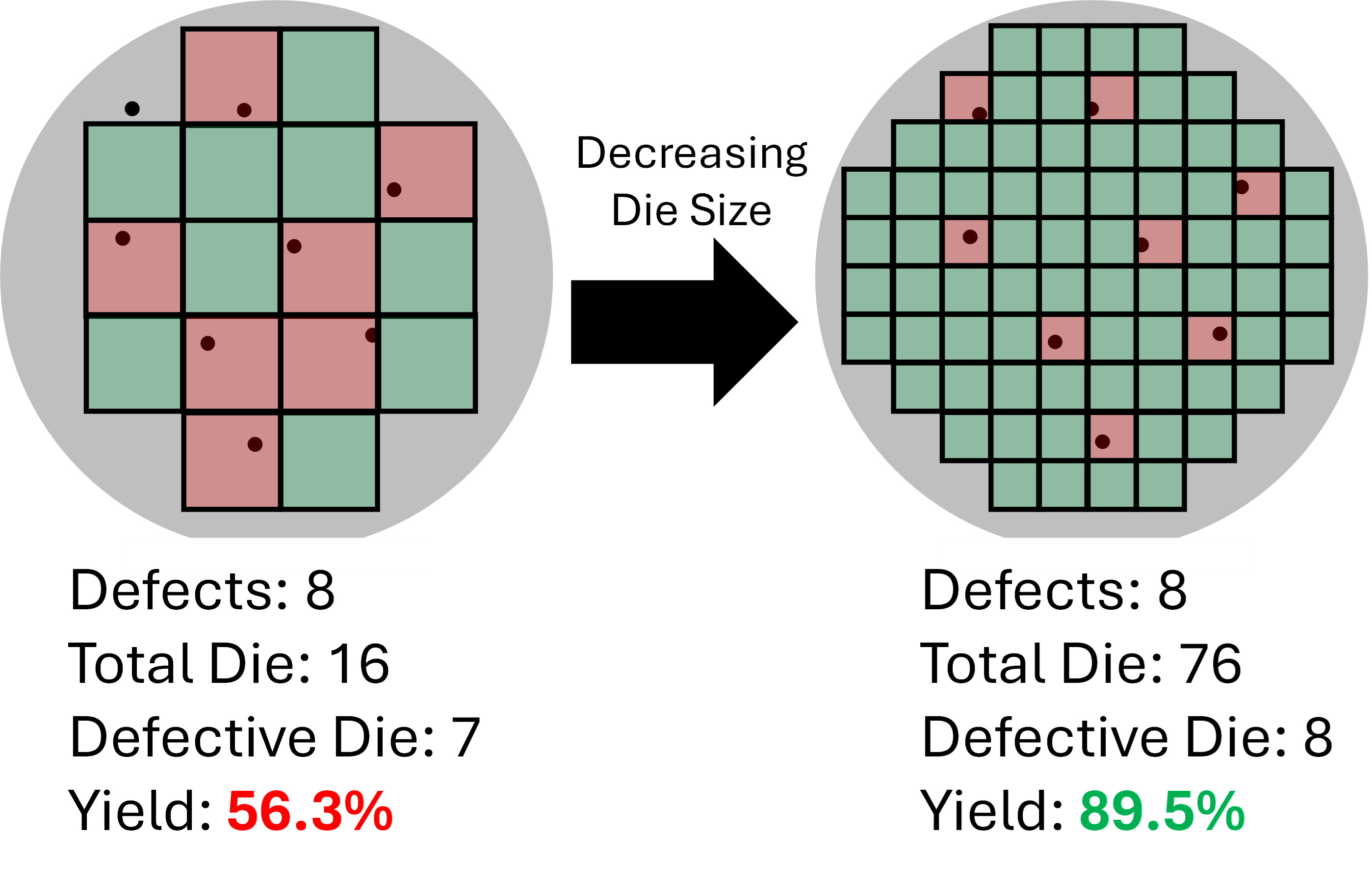
For example, if you have a random distribution of 8 foreign particles across a wafer that only contains 16 dies, the yield will be very low (~50% based on where the particles are located).However, if those same 8 particles are distributed across a wafer with 76 dies, the yield will be much better (~90%).
This serendipitously, and somewhat counter-intuitively, meant that to achieve even higher yields, the physical size of circuits had to decrease. Thus began the age of miniaturization. There was a massive technology push for smaller transistors so that designers could enable higher complexity and performance while fitting all of this into the same or smaller semiconductor area to maintain high yields. This positive feedback loop driving smaller and more complex circuits caused transistor densities to grow from less than 100 transistors/mm2 to well over 200 million transistors/mm2today. We know this progression as Moore’s Law, which was named after Gordon Moore, the early electronics pioneer who predicted the trend. Although transistor architecture and interconnect technology has changed over the years, the fundamental concept of fabricating different types of devices simultaneously on a single wafer remains core to the process.
While the monolithic silicon integrated circuit has revolutionized consumer technology and will continue to drive many markets (especially memory and compute), there are markets that remain underserved by the CMOS chip industry. Silicon as a material has fundamental limits and restricting all the components of a circuit to be made of silicon has its drawbacks.
For example, silicon transistors can’t transmit high frequency signals with high power or efficiency, and silicon as a material does not emit light. These new system requirements placed by the wireless communication and display/lighting domains have led engineers to explore new semiconductor materials to solve these needs. The problem is that while there are new compound semiconductor materials well-suited for these applications, they are fabricated as discrete components before being assembled at the board level with CMOS chips. This assembly is effectively bringing back the problems of the pre-monolithic integration era.
As was evident throughout the history of electronics, there is a limit to the complexity that can be achieved in the system when combining discrete parts. Even in the new chiplet era of CMOS advanced packaging, there are limits to the number, and bandwidths, of the interconnects between different chiplets. In the RF domain, this is due to the length and parasitic nature of the interconnects themselves (i.e. unwanted but also unavoidable performance issues unless the interconnects are very short). These parasitic losses make assembling multichip RF solutions lower performance than is possible with a single chip solution. In the display space, the limit is due to the desire for highly pixelated LED systems such as micro-LED microdisplays. Interconnecting millions of LEDs with silicon driving circuitry using soldered interconnects is a complete reemergence of the tyranny of numbers and must be avoided at all costs.
nsc is unlocking the next era of integration
Sometimes it’s necessary to look to the successful solutions of the past to guide our view into the future. At every instance, integrating different devices into the same manufacturing process allowed a jump to the next level of complexity for the system. For vacuum tubes, it was bringing more elements into the same package for reliability. For transistors, it was monolithic integration and connecting them together on the same wafer to defeat the tyranny of numbers. nsc recognizes the continued value of integration and sees integration of compound semiconductors with CMOS as fundamental to enable new and complex systems for underserved markets. nsc has pioneered a new integration scheme that brings compound semiconductor devices onto CMOS wafers while maintaining compatibility with CMOS manufacturing infrastructure to ensure scalability and rapid adoption. This technology creates a monolithic chip that leverages the maturity of CMOS technology with the necessary compound semiconductor devices to serve emerging markets. While the initial benefits of this integration are obvious, continued development will unearth new possibilities for this ubiquitous platform.
A new age of CMOS +III-V integration will drive RF and optoelectronic systems to levels of complexity that cannot yet be imagined. Just as the personal computer or microprocessor had not been imagined when Kilby and Noyce invented the first integrated circuits, there is a world of opportunity that will be uncovered when integration is applied.
If you are interested in learning more about the benefits of CMOS + III-V integration and how it can enable increased complexity and performance in RF and optoelectronic systems, please contact us at contact@nscinnovation.com.
