

The Future of Displays: Silicon Chips?
For as long as consumer electronics have been around, there have been only 2 successful fully integrated electronic technologies: Silicon integrated circuits (Silicon ICs) and flat panel displays. These technologies are the first and only to print multiple electronic devices into a single package without the need for printed circuit boards. Silicon ICs found numerous uses including computation, memory, and wireless communications, while display manufacturers got extremely efficient at making large format displays filled with “good enough” thin film transistors (TFTs).
Today we’re coming to an interesting juncture in the world of displays. After years of the display roadmap following “bigger is better”, they’re now getting smaller, much smaller. The displays needed for AR and VR glasses in the future are thousands of times smaller than the TVs on your wall. To understand why this creates significant disruption, we need to first understand why flat panel displays succeeded and why the only logical (but unintuitive) next step is to use Silicon chips to replace them.
The Rise of Flat Panel Displays
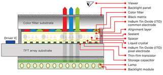
Since the 1990s, flat panel display (FPD) manufacturers have been using technologies such as liquid crystal display (LCD) consisting of a light source, thin film electronic backplane, light blocking liquid crystal pixels, and optical elements like in the diagram below. These components are printed onto huge pieces of glass using photolithography and sputtering and then cut to size to enable many different sized or shaped displays. Critically, all the flat panel display technologies use TFT backplanes whereby the TFTs are manufactured simultaneously leading to an integrated transistor technology similar to Silicon ICs, albeit with lower performance and thus reduced functionalities (hence the “good enough” mentioned earlier).
These flat panel display technologies grew through the digital age and, with them, an entire manufacturing industry developed to produce this amazingly well-received technology. Compared to cathode ray tubes (CRT), flat panel displays were thinner, lighter, and higher definition enabling the age of HD and 4k displays as we know it today. With manufacturing scale, prices dropped throughout the early2000s, eventually surpassing CRTs as the cheapest and most widely adopted display solution. Flat panel displays then found further use cases as consumer portable devices such as laptops created the need for new lightweight and slim displays. This variety in different sizes and resolutions unique to each application, driven by growing consumer need, ability to make generational improvements, and growing fascination with the digital world, fed a manufacturing industry that excelled at both large and small sized displays. These factors also promoted generational advances akin to Moore’s Law scaling in CMOS ICs (720p →1080i → 1080p → 4k).
The Shortcomings of Flat Panel Displays for Next Gen Technologies
While these flat panel displays became better, brighter, and cheaper, one aspect persisted: the displays were always intended to be viewed directly by the human eye. This put a floor on the size of the pixel that made sense to produce. The eye simply can’t resolve pixels smaller than a certain size (~55 µm) at typical display viewing distances. This meant the size of the single pixel was still quite large when compared to state-of-the-art CMOS electronics and more importantly there was and is no real driving force for reducing the pixel size any further. These larger sized pixels mean that the large area flat panel manufacturing equipment and methodologies can be used for all direct‑view consumer applications.
Even to this day if you hold your phone close to your face, you can see these individual pixels each providing a dot of color to create the image you see on the screen. While that pixel is small on the scale of a large device like a TV or phone, pixels in future AR display engines will be much smaller. These AR projector systems have near term benchmarks at pixel sizes of less than 5 µm, well-below the aforementioned floor: ~10× smaller (~100× if we talk about area) than the smallest existing flat panel pixels.
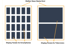
Making this huge jump without any driving force for intermediate improvements seems unlikely. Additionally, the manufacturing equipment used to make LCD and OLED displays excels at making large uniform areas like the size of a TV or computer monitor, not the < 1 cm2 that is estimated to be the size of the future AR display engines. These AR display engines just aren’t fit to be made like these other consumer displays.
The Future of Displays has to be Silicon Chips
Clearly, the incumbent approach (i.e. flat panel displays) isn’t going to work. Does this mean it’s time for scientists and engineers to come up with a completely new manufacturing solution? Well, it isn’t so simple. Making these incredibly small pixels requires a high precision process that is very expensive due to highly specialized equipment and super clean manufacturing facilities. Should we build these expensive facilities that will produce only a single product: AR display engines? Can a single component support an entire manufacturing environment large enough to produce AR display engines on a consumer scale? Is there enough margin present in future consumer AR headsets to justify building an entire manufacturing infrastructure for a single component of a highly complex system.
The answer is most certainly NO to all these questions. So, we turn to the only other existing technology for manufacturing integrated electronic systems: Silicon integrated circuits.
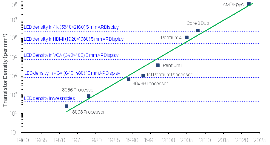
The Silicon manufacturing infrastructure has some key advantages that help to solve the problems outlined above. First, printing small pixels is a no brainer using CMOS manufacturing equipment. As shown in the chart below, the feature density needed for end of roadmap AR displays (the most advanced displays we can presently imagine) is equivalent to the transistor density of microprocessors in 2007. Therefore, CMOS manufacturing infrastructure (even fully depreciated equipment) is more than qualified to fabricate these highly advanced AR display systems.
Second is scalability. This is often a term that is completely abused. Everyone seems to think their technology is “scalable.” It’s more appropriate to look at it through this lens: if tomorrow there is an order for a million units (an incredibly small number for consumer electronics), are there facilities in existence that can feasibly handle the manufacturing of that volume? If you must build new factories to run a proprietary process, the answer is no. CMOS doesn’t have this issue. Global CMOS manufacturing capacity is massive with a global capacity of close to 7.7 million 200 mm wafers per month, and even more for 300 mm (Source: SEMI Fab Outlook to 2026). Each wafer could hold dozens, if not hundreds, of such AR displays. With this infrastructure, hundreds of millions of AR display engines could be produced without even making a dent in global capacity.
nsc is enabling that future
We have one major problem though. CMOS doesn’t emit light, so how can we use it as a display? nsc has solved this problem with the only manufacturable solution that maintains complete end-to-end compatibility with the CMOS manufacturing infrastructure. Our proprietary CMOS + GaN LED process embeds GaN LEDs inside of silicon wafers and uses standard CMOS manufacturing processes to fabricate both LEDs and CMOS devices on the same chip. Our technology takes a unique and patented approach which avoids fab contamination and eliminates the need for dedicated manufacturing equipment not used in other parts of the CMOS fab chain. The result is our PixelatedLightEngine™ (PLE) solution that can be used not only for AR displays, but also for tailored illumination, automotive lighting, and other optoelectronic systems.
If you would like to learn more about how nsc is enabling the future of AR displays or a more detailed understanding of our emerging technology, please contact us at contact@nscinnovation.com.
